Galvanometer motors are pivotal in the precise control of optical components, ensuring that laser scanning systems achieve exceptional accuracy and responsiveness. These motors function by rotating mirrors at different angles, reflecting laser beams to target specific points. Key attributes such as motor torque and speed are crucial in enhancing the accuracy and responsiveness of these systems. High torque guarantees that the mirrors respond accurately to control signals, while optimal speed ensures swift adjustments to the laser beam path. Data from manufacturers consistently indicates that modern galvanometers maintain precision even under high-speed operations. This reliability makes them indispensable in industries where accuracy is paramount.
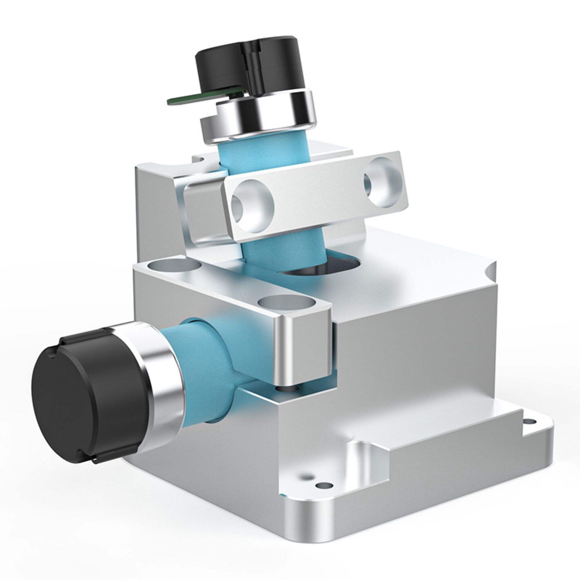
Scanning mirrors in dynamic galvo scanners are essential for achieving high-speed operations, as they direct laser beams swiftly and precisely. The mirrors are typically made from lightweight materials like silicon carbide, which help reduce inertia. Recent advancements in mirror technology have significantly decreased inertia, allowing for quicker response times and smoother operations. When evaluating mirrors, performance metrics such as reflectivity and weight are crucial. Modern mirrors excel in high reflectivity, ensuring minimal loss of laser power and maintaining efficiency. Compared to older technologies, today's mirrors offer superior performance, enhancing the overall effectiveness of galvo scanners.
Closed-loop feedback systems are integral to ensuring precision and minimizing errors in dynamic galvo scanners. These systems operate by continuously monitoring the output and automatically adjusting to any variations in load or operational conditions. This real-time adjustment capability is vital for maintaining consistent performance. Industries that require high precision, such as microelectronics or medical device manufacturing, rely heavily on these systems for quality assurance. The ability of closed-loop systems to adapt swiftly to changes makes them invaluable for applications where precision is non-negotiable, enhancing the reliability of end products.
When comparing digital and analog control architectures, each has specific advantages and applications. Digital control systems are lauded for their flexibility, scalability, and seamless integration with software. These qualities allow for customizable and easily upgradable solutions, particularly beneficial in complex scanning operations. Conversely, analog systems can offer immediate responses due to their simpler architecture; however, they may lack the versatility of digital systems. Emerging trends indicate a preference for digital systems due to their adaptability and capability to handle complex operations more efficiently. Expert insights suggest that, as technology advances, the shift towards digital will continue to gain momentum, offering more robust solutions for dynamic galvo scanning applications.
Sub-micron precision is a critical advancement in the field of microelectronics, allowing for incredibly detailed and precise electronic markings. As electronic components shrink, the need for precision becomes paramount to ensure that each part functions correctly and efficiently. Research has shown that improved precision can significantly boost the performance and reliability of components, which is essential for maintaining the competitiveness of microelectronics products. Recent technological developments, such as high-resolution laser technology, have been pivotal in achieving this level of precision. By refining the mark's exactness on a component's surface, these technologies ensure not only the flawless functionality of the parts but also their longevity.
High acceleration rates, often exceeding 10,000 rad/s², play a crucial role in enhancing the speed and efficiency of laser marking processes. By reaching such speeds, these systems can drastically reduce the time required to mark multiple components, which is beneficial in mass production environments. For instance, case studies have demonstrated how increased acceleration rates directly contribute to shorter production cycles without compromising on the quality of markings. However, maintaining these rates requires careful consideration of system stability to ensure that neither marking precision nor quality is forfeited. Balancing high acceleration with precision engineering makes it possible to maximize productivity while ensuring the durability and accuracy of the marks.
Dynamic galvo scanners are engineered to integrate seamlessly with automated production line systems, streamlining operations significantly. This compatibility allows manufacturers to boost efficiency and achieve substantial cost savings. By incorporating advanced automation, companies can reduce labor costs and human error, leading to optimized workflows. Several industry leaders have successfully integrated dynamic galvo scanners into their production lines, leading to noticeable improvements in output and quality. These integrations often set benchmarks in operational efficiency, showcasing how automated solutions can transform production environments by making them faster and more reliable, thus furthering the benefits of automation in an evolving industrial landscape.
Laser Direct Structuring (LDS) represents a pivotal advancement in modern PCB manufacturing. Traditional methods often lead to significant material waste and inefficiency, but LDS offers a precise solution for creating conductive pathways directly on the substrate. This method involves using laser technology to define circuit patterns without the need for additional etching or layering processes. The advantages are clear: not only is material waste reduced, but production speed and flexibility are improved. Moreover, LDS facilitates complex designs that were previously challenging with conventional techniques. Current applications across various industries underscore its effectiveness, with data illustrating enhanced production efficiency and reduced costs. As the demand for miniaturized electronics grows, LDS continues to be embraced for its capability to deliver intricate designs with fewer environmental impacts.
Wafer-level component identification is crucial in semiconductor manufacturing, ensuring each chip is correctly processed and tracked throughout the production cycle. This identification process plays a vital role in minimizing defects and enhancing yield. By accurately labeling each wafer, manufacturers can pinpoint issues in the production line before they escalate, leading to a more streamlined manufacturing process and higher quality end products. Statistics reveal that establishments employing detailed wafer-level identification achieve notable reductions in defect rates and improved throughput. Expert viewpoints reinforce this, highlighting the technology's capacity to optimize operations and reduce waste. As semiconductor complexity increases, precise identification becomes even more critical in maintaining competitive production standards, ensuring that each component meets stringent performance criteria.
Hermetic seal welding is essential for safeguarding microelectronic components from environmental damage, ensuring long-term reliability and performance. This technique creates airtight seals around sensitive electronics, protecting them from moisture, gases, and other contaminants. Multiple welding technologies are implemented in achieving these seals, including laser welding and ultrasonic welding, each offering unique benefits. Laser welding provides precision and clean seals, while ultrasonic methods allow for fast and energy-efficient production. Case studies from prominent industry leaders exhibit substantial improvements in component reliability, showcasing how hermetic seals have enhanced the lifespan and performance of electronics. These advancements underscore the necessity of adopting advanced welding techniques to meet the demands of modern microelectronics manufacturing, where protection and durability directly impact product success in the marketplace.
In industrial applications, maintaining thermal stability is crucial to ensure consistent performance, particularly in operations that run continuously. The significance of thermal stability lies in its ability to prevent overheating and maintain equipment longevity and operational efficiency. Effective solutions to enhance thermal management include advanced cooling systems and selecting materials with high thermal conductivity. Cooling systems, such as air and water cooling, are commonly used to dissipate excess heat, and materials like copper and aluminum are chosen for their ability to manage heat. Additionally, industry standards emphasize the importance of thermal stability, guiding design and operational protocols to avoid downtime and equipment failure.
Dynamic field calibration plays a vital role in maintaining the accuracy of galvo scanners in high-precision applications. This technique involves continuously adjusting the scanner's operational parameters to ensure that the intended laser path aligns with the actual laser path. Various calibration methods, such as real-time sensor feedback and automated alignment processes, are employed to enhance this precision. These techniques not only improve accuracy but also reduce the time needed for manual calibrations, boosting overall system performance. Research studies indicate significant improvements in system accuracy when dynamic calibration is employed, highlighting its importance in optimizing high-performance scanning systems.
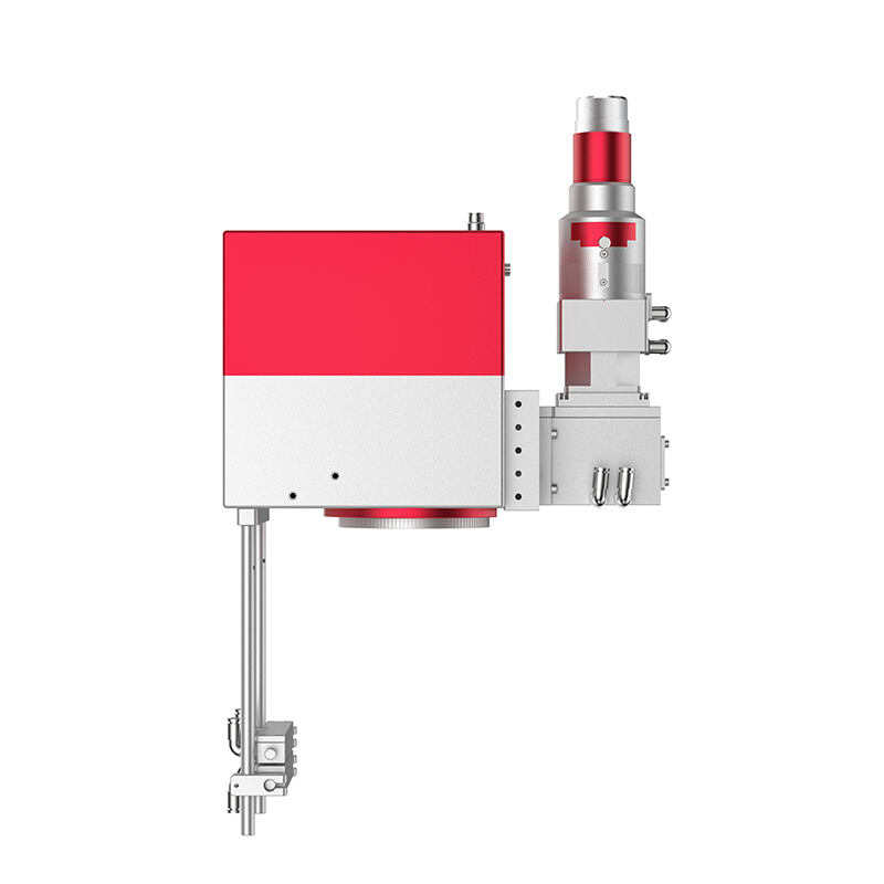
Hybrid motion control integrates the advantages of multiple motion systems, offering superior flexibility and precision over traditional solutions. By incorporating linear stages, hybrid systems significantly enhance the scanning process's flexibility and accuracy, allowing for more complex and precise movements. This integration is beneficial in applications requiring meticulous part positioning and rapid movements, such as in semiconductor or electronics manufacturing. Real-world applications have demonstrated that hybrid systems lead to improved process efficiency and accuracy, providing a competitive advantage in demanding industrial environments. As technology advances, the seamless integration of hybrid motion control will continue to revolutionize precision-based industries.
AI technology is transforming path planning for galvo scanners, a pivotal process for optimizing their efficiency and speed. Footprints from AI-driven algorithms are already evident, showcasing impressive potential improvements. By autonomously adjusting scanner routes, AI can significantly enhance operational speed and precision, lowering the margin for error. Such advancements can enable quick adjustments to variable production conditions, thereby maximizing productivity. For instance, AI algorithms have been successfully integrated into several industries, demonstrating reduced processing times and increased accuracy levels. As more businesses adopt these technologies, the path planning landscape for galvo scanners continues to evolve.
Femtosecond lasers are famed for their precision in manufacturing, capable of producing intricate designs without compromising quality. Integrating these ultrafast lasers into existing galvo systems poses challenges, yet the benefits are compelling. They enable rapid execution of delicate processes like micro-machining and intricate engraving, enhancing production capabilities. Achieving compatibility means addressing synchronization issues and ensuring seamless communication between components. Industry examples, such as aerospace and medical device manufacturing, have successfully embraced this integration, resulting in improved product quality and production efficiency. Adapting to these new technologies is a vital step toward achieving cutting-edge manufacturing standards.
The future of electronics design hinges significantly on advancements in nanoscale feature resolution. As the need for smaller and more efficient components grows, technologies enabling such precise resolutions are becoming increasingly critical. These advancements have implications for the electronics industry, where the demand for compact and powerful devices is ever-expanding. Innovations such as hyper-precise galvo scanners and advanced laser technologies are paving the way for achieving near-microscopic accuracies. Experts forecast that such advancements will revolutionize manufacturing capabilities, setting new benchmarks for product quality and performance. Embracing these changes is crucial for staying ahead in the competitive electronics market.
 Hot News
2026-04-02
2026-04-09
2026-04-08
2026-04-06
2026-04-02
2026-03-31

6th Floor, Block B, Wanhe Technology Building, No. 7 Huitong Road, Guangming District, Shenzhen ,Guangdong Province
Copyright © 2026 Shenzhen Zbtk Technology Co., Ltd. Privacy policy